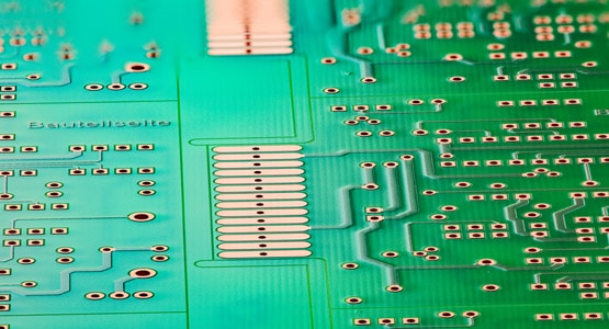
Contact tinning for PCB manufacture
EC iCORE 900 contact tinning is a 2-step process for electroless tin deposition by charge exchange on copper and copper alloys. In the PCB industry, it is used to build a dense, uniform, semi-matt and very solderable tin layer. The process reliably builds up a bright tin layer thickness of > 1 µm. It can be used vertically as well as horizontally. The deposited layers can be stored for 12 months under the known storage conditions.
This process is characterised by its low viscosity, optimum wetting, low surface tension and the finest structures. The highly reliable solder joints demonstrate a very high-quality solder joint. The planarity of the deposition makes the method particularly suitable for the use/processing of BGAs (fine pitch) or µBGAs.
System profile
- Uniform, semi-matt and planar deposition for fine pitch BGA or µBGA placement
- RoHS compliant, as lead-free
- High stability against contamination
- Whisker inhibited
- Low viscosity for optimal wetting
- Stabilised against the formation of Sn(4+)
- Very good solder mask compatibility
Application profile
- Can be applied horizontally and vertically
- All components can be analysed
- Low working temperature
- Very good rinseability
EC SN-iCORE 900 – Chemical tinning
EC SN-iCORE 900 is a process for electroless tin deposition by charge exchange on copper, copper alloy and lead surfaces. It is also suitable for whitening lead or lead/tin coatings. On copper surfaces, bright, smooth tin layers with a layer thickness of about 03. To 1.5 µm are deposited at a working temperature of 58 °C. This allows solderability even after hydrogen de-embrittlement (e.g. 4 horus at 155 °C). The deposition is RoHS compliant.